Research Examples
Fracture propagation and surface reconstruction in Si
(Physical Review B72, 075323 (2005), “Nanoscale structures formed in silicon cleavage studied with large-scale electronic structure calculations: Surface reconstruction, steps, and bending” by Takeo Hoshi, Yusuke Iguchi, and Takeo Fujiwara)
The 10-nm-scale structure formed in silicon cleavage is studied by the quantum mechanical calculations of large-scale electronic structure. The cleavage process was simulated and the results show not only the elementary process of the (experimentally observed) (111-(2x1) surface reconstruction but also several step formation processes. The bendings are observed from the initial (001) plane to (111) -type and/or (110) -type planes, such as (001)->(111)->(110) planes.. These processes are studied by analyzing electronic freedom and compared with scanning tunneling microscopy experiments. The stability mechanism of the (111) -(2x1) cleavage mode is presented beyond the traditional approach with surface energy. In other results, the cleavage path was bent into the experimentally observed planes, owing to the relative stability among cleavage modes. Several common aspects between cleavage and other phenomena are discussed from the viewpoints of non-equilibrium process and 10-nm-scale structure.
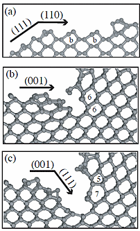
Appearance of well-defined reconstructed surfaces after bending in cleavage path. The figures are drawn by projection from the [1-10] direction. (a) Bending from the (111) plane to (110) plane. After the bending, the buckled (110) surface structures appears, as indicated by b. (b) and (c) Two snapshots of the bending from (001) plane to (111) plane. The resultant (111) plane contains the π-bonded (2x1) structure with seven-membered and five-membered rings, indicated as 7 and 5 in (c).
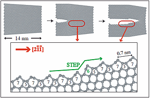
Cleavage process of silicon with (111)-(2x1) cleaved surface.
Helical multi-shell gold nanowires
(Phys. Rev. Letters 99, 125507 (2007) “Two-Stage Formation Model and Helicity of Gold Nanowires” by Yusuke Iguchi, Takeo Hoshi, and Takeo Fujiwara.)
A model for the formation of helical multishell gold nanowires is proposed and is confirmed with quantum mechanical molecular dynamics simulations. The model can explain the magic number of the helical gold nanowires in the multishell structure. The reconstruction from ideal nonhelical to realistic helical nanowires consists of two stages: dissociations of atoms on the outermost shell from atoms on the inner shell (Stage 1) and slip deformations of atom rows generating (111)-like structure on the outermost shell (Stage 2). The elementary processes are governed by competition between energy loss and gain by s and d electrons together with the width of the d band. The possibility for the helical nanowires of platinum, silver, and copper is discussed.
The detailed analysis shows that the mechanism in both Stages 1 and 2 is governed by the d bandwidth and the helical nanowires appear only among metals with a wider d band. The d bandwidth in platinum and gold is commonly wider than that in lighter elements, Ag and Cu. The two-stage model explains why the platinum nanowire can be also formed with helicity.
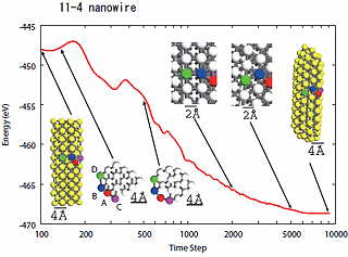
Change of the total energy and the atomic configuration during the formation process of the 11-4 nanowire at 600 K. Red, blue, purple, and green atoms are named A, B, C, and D, respectively. Within 500 MD steps, the atom A was disassociated from inner shell. Between 2000 and 5000 MD steps, the slip between the atom B and D brought the surface reconstruction, and (001) face becomes (111) face.
Elongation growth mechanism of Carbon Nanotube.
(unpublished: “Seeding growth model of carbon nanotubes”, by Shuang Zhang, Takeo Hoshi, and Takeo Fujiwara)
The elongation growth processes of drawing out a seed carbon nanotube from carbon fluid are studied by molecular dynamics simulations. The range of suitable growth conditions of drawing velocities, carbon fluid densities and temperatures are given, which show that the low temperature and density zone of catalytic chemical vapor deposition method can be expanded, and a much higher growth velocity could be achieved by mechanical control. Sometimes, we observe that the defects in grown nanotube are healed by attached carbon clusters, and a mechanism for defect-free product is discussed. The Czochralski-like approach is proposed to produce carbon nanotube “single crystal” labeled by special (n,m) by cloning a seed nanotube, and the (n,m) crystal can be used as template to mass produce same materials. We simulate the process of fabricating a Y junction with two nanotubes, and propose a route towards mass production of wirelike networks of carbon nanotubes.
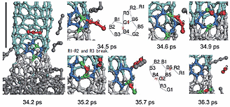
Atomic configurations during the defect healing process observed in growth process (a) A series of configurations during the process. The simulation times are noted. The blue atom signed by number n is denoted by B(lue)n, similarly, e.g. G(reen)1 and R(ed)1.